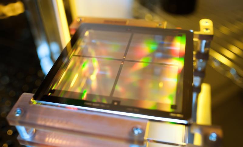
In the dynamic world of semiconductors, photomask inspection has become a crucial element of quality control, enabling defect detection at the microscopic level. A photomask, also known as a reticle, is a template used in the lithography process to project circuit patterns onto semiconductor wafers. As chip designs grow increasingly complex, even the smallest imperfection on a photomask can result in critical manufacturing defects. Hence, the photomask inspection market has seen notable growth and innovation, evolving as a vital pillar in semiconductor production.
This article provides essential market insights into photomask inspection, exploring the latest trends, technological breakthroughs, regional outlook, and future opportunities that define this space.
Evolving Role of Photomask Inspection in Semiconductor Manufacturing
Photomask inspection systems are used to identify defects such as particles, pattern defects, and phase shifts on photomasks before they are used in chip fabrication. As the industry shifts toward sub-5nm technology nodes and integrates EUV (Extreme Ultraviolet) lithography, the role of photomask inspection is becoming increasingly vital.
Recent insights show that photomask inspection is no longer limited to a supporting function—it is now an integral part of the design-to-manufacturing loop. With increased sensitivity requirements, inspection tools must balance speed, accuracy, and cost-efficiency to meet the high throughput needs of modern fabs.
Key Market Trends and Technological Insights
1. Rise of EUV-Compatible Inspection Tools
EUV lithography is a major enabler of next-generation chips. However, EUV masks have multilayer reflective structures that introduce new defect types. Advanced photomask inspection tools equipped with actinic inspection technology (using EUV wavelength light) are being developed to address these challenges. Companies like KLA Corporation and Lasertec are leading this space with next-gen equipment designed specifically for EUV defect detection.
2. Artificial Intelligence and Machine Learning Integration
AI-driven inspection is transforming how photomask defects are detected and classified. By training algorithms on historical defect data, systems can now differentiate between critical and non-critical defects, reducing false alarms and optimizing yield. Machine learning also supports predictive maintenance and improves overall tool efficiency.
3. High-Resolution E-Beam Inspection Systems
As optical inspection faces limitations in resolution, e-beam (electron beam) inspection is gaining popularity for identifying nanoscale defects. These systems are particularly effective for logic and memory chips at advanced nodes. However, their slower speed compared to optical tools remains a challenge, making hybrid solutions increasingly attractive.
Regional Market Insights
The photomask inspection market is globally distributed, with each region exhibiting unique strengths and investment strategies:
-
Asia-Pacific remains the largest and fastest-growing region, with Taiwan, South Korea, Japan, and China housing major fabs and photomask manufacturing facilities.
-
North America, led by the U.S., is witnessing growth fueled by the CHIPS Act, which aims to bolster domestic semiconductor capabilities.
-
Europe is focusing on strengthening its semiconductor supply chain through strategic partnerships and government funding, especially in automotive and industrial chip production.
These regional dynamics are fostering both competition and collaboration, creating fertile ground for photomask inspection vendors to expand their market presence.
Major Players and Competitive Landscape
The market is currently dominated by a few key players who continue to innovate and collaborate with semiconductor giants:
-
KLA Corporation: Offers a comprehensive suite of optical and e-beam inspection systems and is a leader in both DUV and EUV inspection.
-
Lasertec Corporation: Pioneers in EUV mask inspection systems, critical for next-gen nodes.
-
Applied Materials and ASML: Invest heavily in integrated lithography and inspection solutions.
These companies are not only providing cutting-edge inspection tools but also offering data analytics and software support for yield improvement.
Market Challenges and Constraints
Despite rapid growth, the photomask inspection market faces several challenges:
-
High capital expenditure for acquiring and maintaining advanced inspection equipment
-
Technological complexity of EUV mask inspection and actinic imaging
-
Lack of skilled operators and engineers familiar with next-gen systems
-
Supply chain disruptions impacting semiconductor equipment components
Overcoming these hurdles requires ongoing R&D, government support, and strategic industry partnerships.
Future Opportunities and Strategic Outlook
The future of photomask inspection lies in scalable solutions, cloud-integrated analytics, and smart factory adoption. As fabs become more automated, inspection tools must integrate seamlessly with production lines and offer real-time data for decision-making.
Emerging opportunities also include:
-
Inspection systems for compound semiconductors and heterogeneous integration
-
Adoption of edge AI in inspection tools for instant classification
-
Expansion in fabless and outsourced semiconductor assembly and test (OSAT) companies seeking inspection-as-a-service
Conclusion
The photomask inspection market is entering a transformative phase driven by innovation, integration, and industrial demand. From AI-powered tools to EUV-specific inspection systems, the market is responding dynamically to semiconductor scaling challenges. Regional investments, government initiatives, and competitive innovation will continue to define this space, offering exciting opportunities for both established players and emerging tech firms.
Understanding these market insights is essential for stakeholders aiming to capitalize on growth trends and shape the future of semiconductor manufacturing.