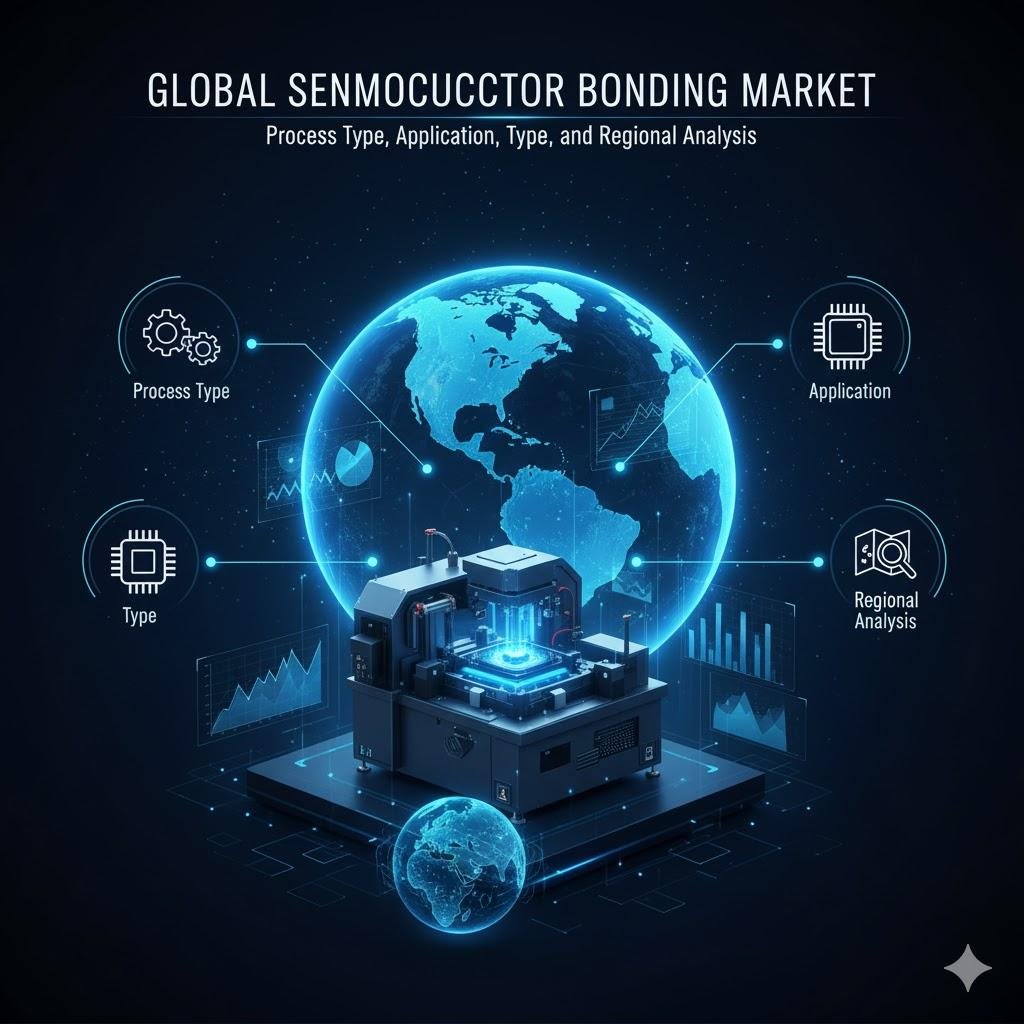
Global Semiconductor Bonding Market: Process Type, Application, Type, and Regional Analysis (2024–2032
The Global Semiconductor Bonding Market is a critical and rapidly evolving segment of the semiconductor manufacturing ecosystem. Bonding is a fundamental process used to permanently attach a die to a substrate, package, or another die, enabling electrical connectivity, mechanical stability, and thermal management. The market is being propelled by the relentless demand for smaller, more powerful, and energy-efficient electronic devices, the rise of 3D integrated circuits (ICs), and the expansion of advanced packaging technologies.
According to Credence Research the Semiconductor Bonding Market was valued at USD 950.6 million in 2024 and is anticipated to reach USD 1,265.3 million by 2032, growing at a CAGR of 3.64% during the forecast period.
Source: https://www.credenceresearch.com/report/semiconductor-bonding-market
1. Market Segmentation: Detailed Analysis
1.1. By Process Type
This is a primary segmentation, distinguishing the fundamental technology used in the bonding process.
- Die Bonder:
- Dominant and Critical Segment: This process involves attaching a semiconductor die (chip) to a package substrate or lead frame. It is one of the most common and essential steps in assembly and packaging.
- Key Drivers: The massive volume of chips packaged for everything from consumer electronics to automotive systems. Advancements in precision and speed for handling ultra-thin and large dies are crucial.
- Sub-types: Includes epoxy die attach, eutectic die bonding, and soft solder die attach.
- Wafer Bonder:
- High-Growth Technology Segment: This process involves bonding an entire wafer to another wafer or a carrier substrate. It is a key enabler for advanced 3D packaging and MEMS (Micro-Electro-Mechanical Systems) manufacturing.
- Key Drivers: The industry's shift towards 3D ICs, 2.5D/3D packaging, and More-than-Moore approaches. It allows for higher performance, reduced form factors, and heterogeneous integration (combining different chips, e.g., logic and memory).
- Sub-types (by method):
- Direct/Fusion Bonding: Creates a permanent, direct covalent bond between two wafer surfaces.
- Adhesive Bonding: Uses an intermediate polymer layer.
- Metal-Thermo Compression Bonding: Used for high-density interconnects, crucial for 3D stacking.
- Anodic Bonding: Primarily used for MEMS, bonding glass to silicon.
1.2. By Application
This defines the key end-use industries and products driving the demand for bonding technologies.
- MEMS and Sensors:
- Mature and Significant Segment: Bonding is fundamental for creating the sealed cavities and structures required for MEMS devices like accelerometers, gyroscopes, pressure sensors, and microphones.
- Key Drivers: Proliferation of IoT devices, automotive safety systems, and smart consumer electronics.
- RF Devices:
- Includes filters, power amplifiers, and switches for smartphones, base stations, and wireless connectivity. Advanced bonding ensures signal integrity and performance.
- CMOS Image Sensors (CIS):
- High-Growth Segment: Stacked CMOS image sensors, where the pixel array is bonded to a logic wafer, rely heavily on wafer bonding.
- Key Drivers: The demand for high-resolution cameras in smartphones, automotive ADAS, and medical imaging.
- 3D IC Stacking & Advanced Packaging:
- The Frontier of Innovation: This is the fastest-growing application segment. It includes technologies like Through-Silicon Via (TSV) and Hybrid Bonding.
- Key Drivers: The need for superior performance in AI accelerators, high-bandwidth memory (HBM), and data center chips, where traditional scaling is becoming challenging.
- LED and Optoelectronics:
- Involves bonding LED dies to substrates for thermal management and light extraction.
- Logic and Memory:
- Traditional and high-volume applications for die bonding in processors, DRAM, and NAND flash memory.
1.3. By Type
This segment categorizes the market based on the technique or principle used.
- Die to Wafer (D2W):
- Involves bonding singulated dies onto a wafer. Offers flexibility for heterogeneous integration.
- Wafer to Wafer (W2W):
- Involves bonding two entire wafers together. Highly efficient for homogeneous structures but requires perfect yield across both wafers.
- Die to Die (D2D):
- A specialized process for stacking individual dies on top of each other.
2. Regional Analysis (2024–2032)
- Asia-Pacific (APAC):
- Undisputed Market Leader: Dominates both in production and consumption, accounting for the largest market share (>60%).
- Key Drivers: The presence of the world's largest semiconductor foundries (TSMC in Taiwan, Samsung in South Korea), major OSAT (Outsourced Semiconductor Assembly and Test) providers (e.g., in China, Malaysia, Vietnam), and a massive electronics manufacturing base (China, Japan, South-East Asia). Government initiatives for semiconductor self-sufficiency in China and India are providing further impetus.
- North America:
- Innovation and R&D Hub: Holds a significant share, driven by the presence of leading fabless semiconductor companies (AMD, NVIDIA, Qualcomm), IDMs (Intel), and equipment manufacturers.
- Key Drivers: Heavy investment in R&D for next-generation packaging and bonding technologies (e.g., hybrid bonding). The US CHIPS and Science Act is catalyring domestic manufacturing and associated supply chains, including advanced bonding.
- Europe:
- Strong in Niche and Industrial Applications: A well-established market with a focus on quality and precision.
- Key Drivers: Leadership in automotive semiconductors (Germany, France), industrial electronics, and MEMS sensors (STMicroelectronics). The European Chips Act is aiming to bolster the regional semiconductor ecosystem.
- Rest of the World (Latin America, Middle East & Africa):
- Emerging Markets: Currently smaller but with growing potential.
- Key Drivers: Increasing local electronics assembly and government efforts to attract high-tech manufacturing investments.
3. Key Market Drivers and Trends
- Primary Drivers:
- Demand for Miniaturization and High Performance: The end of Moore's Law scaling is pushing the industry towards 3D integration, where bonding is paramount.
- Proliferation of AI, HPC, and 5G: These technologies require advanced packaging solutions like CoWoS and HBM, which are impossible without sophisticated wafer-level bonding.
- Growth of Automotive Electronics: The increase in electric vehicles (EVs) and autonomous driving systems demands reliable and robust semiconductor packages for sensors and power electronics.
- Expansion of the Internet of Things (IoT): Billions of connected devices require small, low-power, and cost-effective chips, driving volume demand for both die and wafer bonding.
- Key Trends:
- Hybrid Bonding: This is the most significant trend, moving from bump-based connections to direct copper-to-copper bonding, enabling ultra-fine pitch and higher performance for 3D stacking.
- Thermo-Compression Bonding (TCB): Gaining traction for high-density die-attach applications, especially in heterogeneous integration.
- Advanced Materials: Development of new underfills, adhesives, and interface materials to manage thermomechanical stress and improve reliability.
- Automation and AI in Bonding Equipment: Integration of machine vision and AI for real-time process control, defect detection, and yield improvement.
4. Challenges and Restraints
- High Capital Investment: Advanced bonding equipment, especially for wafer-level and hybrid bonding, is extremely expensive.
- Technical Complexity: Processes like hybrid bonding require near-perfect surface planarity and cleanliness, posing significant engineering challenges.
- Supply Chain Vulnerabilities: Dependence on specific regions for equipment and materials can lead to disruptions.
- Skilled Labor Shortage: Operating and maintaining advanced bonding tools requires highly specialized engineers and technicians.
5. Competitive Landscape
The market is characterized by a mix of established global players and specialized technology providers.
- Leading Equipment Vendors: Besi, ASMPT, and Kulicke & Soffa (K&S) are dominant in die bonding. EV Group (EVG) and SUSS MicroTec are leaders in wafer bonding equipment.
- Integrated Device Manufacturers (IDMs) and Foundries: Companies like Intel, Samsung, and TSMC are driving process innovation internally, often co-developing tools with equipment makers.
- Strategic Focus: Key competitive strategies include heavy R&D investment in hybrid bonding and TCB, forming strategic partnerships with leading chipmakers, and providing comprehensive process solutions (equipment + materials + process support).
In conclusion, the Global Semiconductor Bonding Market is transitioning from a back-end assembly process to a frontline enabler of semiconductor innovation. The shift towards 3D integration and heterogeneous integration is placing bonding technology at the heart of the industry's future, ensuring its critical role and dynamic growth throughout the 2024–2032 forecast period.
Source: https://www.credenceresearch.com/report/semiconductor-bonding-market